Memory Levels
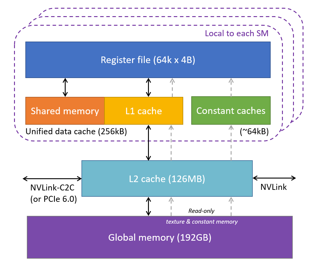
Compared to a CPU core, a streaming multiprocessor (SM) in a GPU has many more registers. For example, an SM in the NVIDIA Blackwell B200 has 65536 registers in its register file. Taken as a whole, its register file is larger in terms of its total capacity than a CPU's, too, despite the fact that the SM's 4-byte registers hold just a single float, whereas the vector registers in an Intel AVX-512 core hold 16 floats.
But CPUs have an advantage in total cache size. Every Intel CPU core comes with L1 and L2 data caches, and the size of these caches plus its share of the shared L3 cache is easily larger than the equivalent caches in a GPU, which has nothing beyond a shared L2 cache. The figure shows the full picture of the memory hierarchy in the Blackwell B200. The roles of the different caches and memory types are explained on the next page.
(Based on diagrams by NVIDIA and Citadel at GTC 2018)
Arrows in the above diagram show how the layers of memory are linked together. Depending on where the data start, they may have to hop through several layers of cache to enter the registers of an SM and become accessible to the CUDA cores. Global memory (including areas for local, texture, and constant memory) is by far the largest layer, but it is also furthest from the SMs.
Clearly it would be favorable for 4-byte operands to travel together in groups of 32 as they move back and forth between caches and registers and CUDA cores. Why? A 32-wide group is exactly right to supply a warp of 32 threads, all at once. Therefore, it makes perfect sense that the size of the cache line in a GPU is 32 x (4 bytes) = 128 bytes.
Notice that data transfers onto and off of the device are mediated by the 126MB L2 cache. In most cases, the incoming data will proceed from the L2 into the large global memory of the device. This is because in NVIDIA architectures, all the data traffic basically flows through the L2 cache. The memory controllers are connected to the cache; so is the connection to the host. And all SMs are connected through the same L2 cache.
A way to think about it is that the L2 cache is a proxy for device memory. Device memory accesses go through the L2 cache... the oldest data in the cache will be written out to device memory when it needs to make space for new data, according to the cache eviction policy.
CVW material development is supported by NSF OAC awards 1854828, 2321040, 2323116 (UT Austin) and 2005506 (Indiana University)