Memory Access Times
The storage units that are nearest of all to the CPU cores are the registers, which hold data that the functional units can operate on directly. This is where your data come together with the instructions from your code. Really, instructions are just another form of data, so they have their own caches. (Instruction caches have not been depicted, but they too are important to overall performance.) There is no delay in accessing the data that are in registers.
Registers are given architecture-specific names and can be programmed directly by using the architecture's assembly language. If you like, you can see what registers are being used when by looking at the assembly output when you compile your code. Most compilers have the option of generating assembly-language code before translating it to machine code.
If any needed data are not present in the registers, then they must be retrieved from further out in the memory hierarchy. The simplest model for the retrieval cost at each level is T = S/B + L, where T is time, S is size, B is bandwidth, and L is latency. Latency is therefore the cost that must be paid for fetching even the tiniest amount of data. The combined cost is cumulative, since the data will be copied into progressive cache levels as it makes its way to the registers.
Looking at the read bandwidth and latency measurements done on Skylake server chips, below, we see that bandwidth is roughly cut in half at each succeeding level of the hierarchy, while latency essentially quadruples at each level as one progresses away from the registers. In other words, the speed and initiation time of memory accesses become exponentially worse as one moves out in memory level. Performance penalties can clearly start to add up quickly in code that is not optimized with good memory locality in mind. This is why it is best to keep computations operating as much as possible on data that reside in the fastest levels of the memory hierarchy.
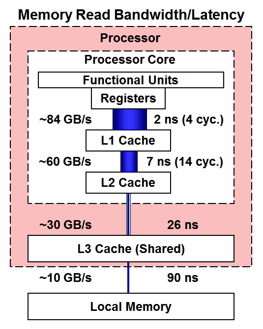
As a reference for the read bandwidth values noted above, see the Sandia report by Hammond, Vaughan, and Hughes 2018, which presents results from a Skylake configuration identical to what is found in Stampede3. Latencies are from results on a slightly different Skylake, the Xeon Platinum 8176, which differs from the Xeon Platinum 8160 in Stampede3 only in core count (28 vs. 24).
Finally, let's briefly expand our view of the memory hierarchy to include both of the Skylake processors on a Stampede3 SKX node, as well as the node's connections to other Stampede3 nodes. One possible measure of "distance" is the aggregate, ideal bandwidth for all available channels that link a processor (and all its cores) either to its local memory or to a different node. The figure below shows that the dual processors should be considered very close together, while the other nodes are relatively far away in terms of memory access speed. Other nodes would be even farther away if latency rather than bandwidth over Omni-Path were the relevant metric.
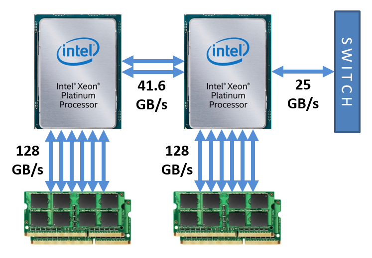
Bandwidths appearing in the above figure are theoretical peak speeds.1 Measured memory bandwidths on SKX nodes generally reach 75-80% of ideal, provided that most cores are active. Measured bandwidths for the other types of links are closer to ideal.2
1. Ideal bandwidths on SKX nodes are computed as follows. (a) Based on information in the Stampede3 User Guide, TACC populates all 6 memory channels on 2 sockets with two 8 GB DDR4-2666 modules apiece, resulting in 192 GB per node. Peak rate per socket is thus (6 channels) x (21.3 GB/s) = 128 GB/s. (b) Sockets are coupled by 2 Ultra Path Interconnect (UPI) links, each capable of 20.8 GB/s full duplex, for a sum of 41.6 GB/s. Note that the Xeon Platinum 8160 can support 3 UPI links, but only 2 are enabled in Stampede3 nodes (MacCalpin 2021, footnote 2). (c) An Intel Omni-Path Host Fabric Interface Adapter rated for 100 Gb/s requires a PCIe3 x16 slot; such a slot has a theoretical peak of 16 GB/s in each direction, but it is limited to 12.5 GB/s by the adapter.^
2. Measurements for Stampede3 SKX nodes have been published by TACC (Figs. 4 and 13). The combined read/write memory speed is found to be ~100 GB/s to memory on the same socket, and ~45 GB/s to memory on the opposite socket, assuming all 24 cores of one processor are active (24 threads). Between nodes, Intel Omni-Path is observed to achieve its advertised speed of 12.5 GB/s (100 Gb/s) for a single MPI sender and a single MPI receiver. These published figures are consistent with typical data rates for each type of connection.^
CVW material development is supported by NSF OAC awards 1854828, 2321040, 2323116 (UT Austin) and 2005506 (Indiana University)