Memory Hierarchy
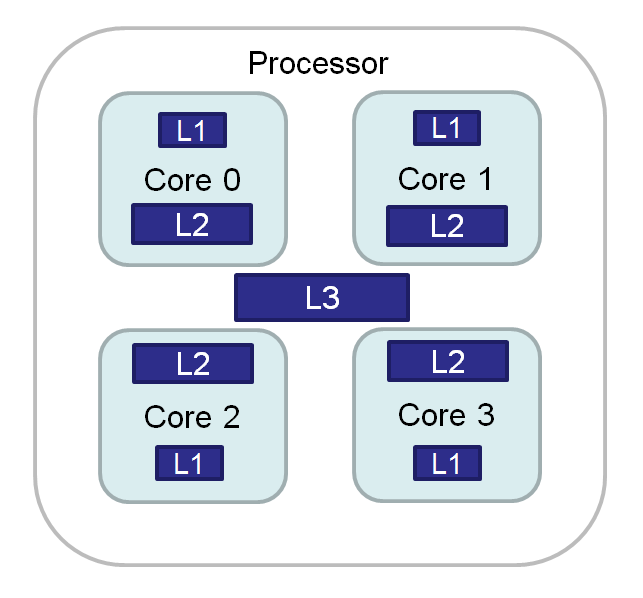
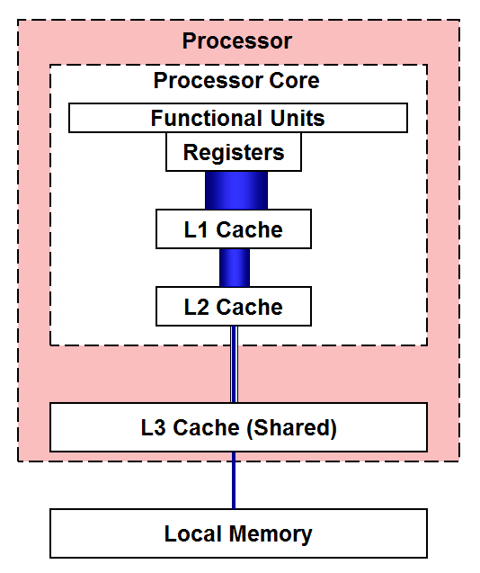
In a typical multi-core processor, all the computing action happens in the functional units inside the cores,. Thus, any data that are to be operated upon must first be brought into proximity to these units. However, loading data from main memory is slow, because memory modules are physically distinct from the processor chip. All microprocessors therefore have various levels of cache memory built into the chip. For example, Intel Xeon Scalable Processors have three levels of cache, with Level 1 (L1) being closest to the functional units. As the diagram below illustrates generically, the L1 and L2 caches are specific to each core in a multi-core processor, whereas the L3 cache is shared among all cores.

The levels of cache memory are arranged in a hierarchy. Data move up in the hierarchy when they are about to be used, and are allowed to migrate further away if they are not used. This is sensible because data that are used once are more likely to be used again; likewise, data that have been used frequently are more likely to remain so in the future. Accordingly, the data in the L1 (closest) cache are reachable with relatively high bandwidth (speed) and low latency (delay). Less-frequently accessed data are stored in more distant locations, all the way out to main memory. This type of cache hierarchy exists in any modern processor.

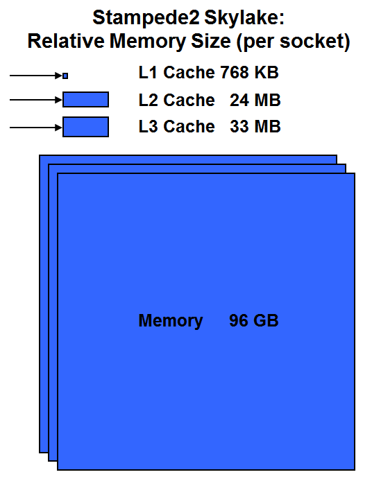
While the speed of data retrieval does fall off markedly with distance, bear in mind that the pools of distant/slow memory can be vastly larger than the close/fast memory. The figure below illustrates the size of the various memory levels, including the directly attached memory, for an Intel Xeon Skylake processor (where "Skylake" is the Intel code name for the first generation of Xeon Scalable Processors). Sizes shown below are the totals per processor, or "per socket", referring to the plug-in locations for the processors. While all memory levels are accounted for, note that the main memory boxes are not really to scale: it would take ten times as many blue boxes of memory (30 in all) to represent 96 GB, and twice that number to represent the shared RAM in a dual-processor node. However, the figure should give you an idea of the disparity in size between main memory and the caches.

As mentioned, the memory hierarchy extends beyond a single processor and the RAM attached to that one socket. In TACC's Stampede3 cluster, for example, a basic Skylake or "SKX" compute node possesses two sockets, each with 24 cores and 96GB of RAM, with all RAM accessible to both sockets (48 cores, 192 GB). You won't be surprised to learn that a processor can access the RAM in its own socket more quickly than it can access the RAM on the other socket. However, the platform is designed with latency low enough and bandwidth high enough between the sockets to make that distinction not as significant as it seems, at least not for common patterns of memory access.
At the very farthest end of hierarchy is RDMA, or remote direct memory access to other nodes of a cluster, followed by spinning disk and tape storage. We do not focus on these more remote elements here. Suffice it to say that in terms of performance, trying to synchronize processes via, e.g., file I/O is not likely to be a good choice. In any event, in this topic we will be concerned primarily with the addressable, physical memory of a single node.
CVW material development is supported by NSF OAC awards 1854828, 2321040, 2323116 (UT Austin) and 2005506 (Indiana University)