V100 Memory & NVLink 2.0
The Tesla V100 features high-bandwidth HBM2 memory, which can be stacked on the same physical package as the GPU, thus permitting more GPUs and memory to be installed in servers. The V100s in TACC Longhorn have eight memory chips per HBM2 stack, and four stacks, yielding 32 GB of GPU memory in each device. This configuration provides 900 GB/sec of peak memory bandwidth across the four stacks.
Data integrity is important in scientific computing, and the CPUs of HPC systems typically have ECC (error correction code) memory as a guard against data corruption. This feature is found in NVIDIA's GPGPU devices as well, and it is a property of both the Tesla V100 and the Quadro RTX 5000.
Most often, data starts out on the host and must be transferred to the memory on the device. Such memory transfers may be initiated explicitly, but it is also possible to do this through Unified Memory, a single memory address space that permits applications to allocate and access a common set of data from code running on either CPUs or GPUs.
Allocating Unified Memory is straightforward: typical calls to malloc() or new are simply replaced with calls to
cudaMallocManaged(). The resulting pointer provides access to the data from any processor.
CUDA system software works with the hardware to take care of migrating the requested memory pages
to the physical memory of the accessing processor, whether it is on the host or the device.
Several streams of memory transfers are typically initiated on the CPU side, so that some GPU kernels can start doing their computations while other kernels wait for data. This is true of explicit transfers as well as those done implicitly through Unified Memory.
Host-to-Device and Device-to-Device Transfers
The speed at which data can be transferred from the host to the device and back is set by the type of interconnect. In most cases, GPU devices are inserted into expansion slots in their hosts, and the number of PCIe lanes in the slot determines the peak bandwidth. Commonly, the Tesla V100 is connected to the host by 16 lanes (x16) of PCIe3, each capable of 1 GB/s in each direction, providing an overall bidirectional bandwidth of 32 GB/s.
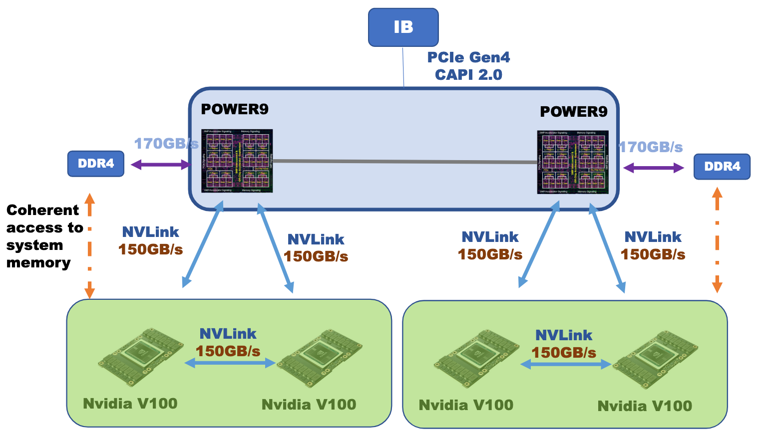
TACC Longhorn, however, was built around IBM POWER9 processors, which at the time were the only CPUs that could communicate directly with GPUs using NVIDIA's NVLink 2.0 technology. NVLink was originally developed to provide dramatic improvements in bandwidth between GPU devices, but in IBM servers it was further used to remove the potential PCIe bottleneck between CPUs and GPUs. The figure below shows the speeds of the bidirectional NVLink 2.0 connections within a Longhorn node.

Source: IBM presentation at GTC 2018
If each POWER9 processor had just one V100 attached to it, that single connection could reach the full peak bidirectional bandwidth of 300 GB/s. As it is, the bandwidth to one of the processors is split between two attached GPUs to give 150 GB/s to each, and these GPUs are in turn attached to one another with a 150 GB/s link. The second processor in each node has a similar arrangement with 2 attached GPUs of its own.
The L2 cache plays a key role in moving data from the host to the device's global memory, as well as from global memory to the SMs and CUDA cores. The full memory hierarchy and the properties of the various caches within it were detailed in the GPU Memory topic.
In conclusion, the high flop rate of a GPU is only meaningful if the data rate from and to the host can keep up. NVLink 2.0 and HBM2 may therefore be crucial in allowing data-heavy applications to use the full speed of the V100. In any case, it is a viable option for applications that need FP64 precision.
CVW material development is supported by NSF OAC awards 1854828, 2321040, 2323116 (UT Austin) and 2005506 (Indiana University)