Inside a Blackwell B200 SM
We now zoom in on one of the streaming multiprocessors depicted in the diagram on the previous page. Each Blackwell B200 SM gets its processing power from:
-
Sets of CUDA cores for the following datatypes
- 128 FP32 CUDA cores
- 128 INT32 CUDA cores
- 64 FP64 CUDA cores
- 4 Tensor Cores (5th generation)
- 4 Special Function Units
- 4 Texture units
In general, an SM is subdivided into 4 processing blocks, as shown in the figure. This allows for greater flexibility in scheduling. The CUDA cores can be scheduled so that on every clock cycle, either 4 separate warps of FP32 or INT32 can be processed, or 2 warps of FP64 (or possibly some combination of these).
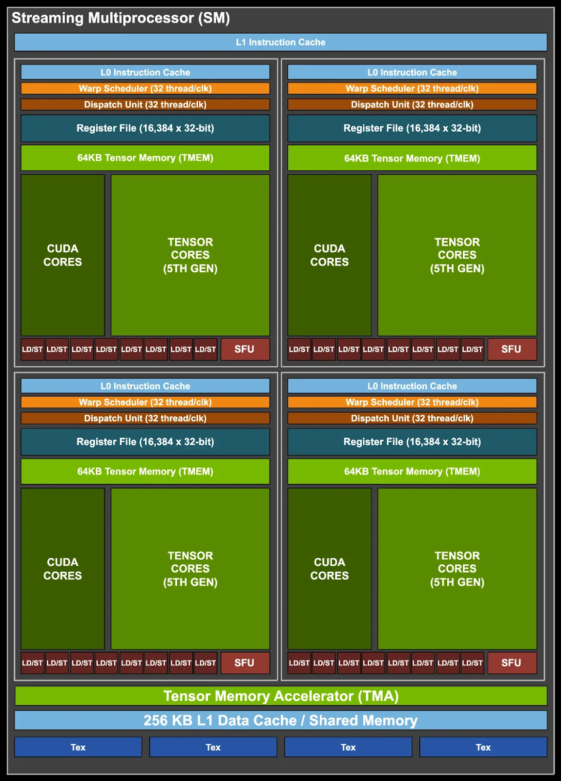
Source: Chips and Cheese
Data are supplied to the main part of this hardware through 32 Load/Store units, as shown at the bottom of each processing block:
- Loads go into the ample 64 KB register file or the 64 KB tensor memory (TMEM) associated with each processing block. A Blackwell B200 SM therefore has, in total, 256 KB of register memory and 256 KB of TMEM.
- Stores, on the other hand, are generally pushed out to the 256 KB L1 data cache. From there, they can propagate to the globally shared L2 cache, then into global memory. Note that the L1 cache size can be adjusted downward to make room for special "shared memory" within the SM, where each data item is accessible to any thread.
Data are loaded into the tensor cores through the special "tensor memory accelerator" (TMA), which can do bulk asynchronous loads independently, thereby taking pressure off the CUDA cores.
CVW material development is supported by NSF OAC awards 1854828, 2321040, 2323116 (UT Austin) and 2005506 (Indiana University)