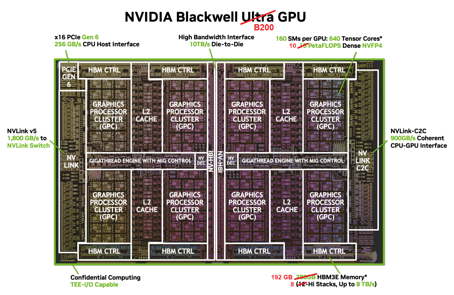
Blackwell Chip Diagram
Each of the two NVIDIA Blackwell accelerators in the Grace Blackwell Superchip is a B200 GPU. The B200 is designed to provide significant speedups to deep learning algorithms and frameworks, while also offering superior number-crunching power for HPC applications. The B200 is unique among NVIDIA's offerings in that it consists of a pair of silicon chiplets or dies joined along one edge by a 10 TB/s link, which allows the pair of dies to function as a single chip.
As with NVIDIA's previous generations, the Blackwell B200 GPU consists of many Streaming Multiprocessors (SMs) arranged into a loose hierarchy. The SMs are paired into Texture Processing Clusters (TPCs), which are in turn grouped into GPU Processing Clusters (GPCs). Each of the two B200s found in Grace Blackwell contains 160 SMs partitioned into 8 GPCs. The Blackwell's overall layout is depicted in the "die shot" below; the figure actually shows the Blackwell B300 or "Ultra" model, but the layout of the B200 is practically identical, differing in just a few respects as noted.
Source: NVIDIA Developer Blog
The higher-level organization into graphics and texture processing clusters is really only relevant to graphics applications. But in case you were counting, each of the 8 GPCs above contains exactly 20 SMs (in 10 TPCs), for a total of 8 × 20 = 160 SMs.
Links to other system components are found at the edges of the above chip diagram. The long bar on the right represents the NVLink-C2C connection to the host with 900 GB/s bandwidth. The long bar on the opposite edge contains much faster NVLink bridges that lead to other NVIDIA devices with 1.8 TB/s bandwidth. On the top and bottom edges are the eight 512-bit memory controllers (4096 bits total) that connect the entire array of SMs to the device's 192 GB of HBM3e high bandwidth memory. The role of the central L2 cache memory will be described later.
CVW material development is supported by NSF OAC awards 1854828, 2321040, 2323116 (UT Austin) and 2005506 (Indiana University)